IBM Debuts World's First Sub-1 Nanometer Chip Technology
Built with revolutionary "nanostack" 3D chip architecture, IBM's sub-1 nm chip to propel semiconductor industry forward for the next decade
YORKTOWN HEIGHTS, N.Y., June 25, 2026 /PRNewswire/ -- IBM (NYSE: IBM) today unveiled a major semiconductor breakthrough with the introduction of the world's first sub-1 nanometer (nm) chip technology, featuring a revolutionary transistor architecture at the 0.7 nm, or 7 angstrom node. The achievement marks a landmark moment for an industry facing the physical limits of traditional chip scaling. Semiconductors play critical roles in everything from computing, to appliances, to communication devices, transportation systems, and critical infrastructure.
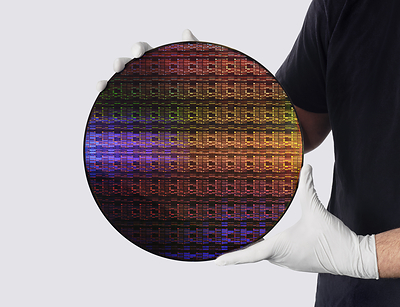
IBM's new sub-1 nm chip packs nearly 100 billion transistors onto a chip the size of a fingernail, nearly twice the density of IBM's 2 nm chip, unveiled in 2021. Enabled by a series of structural and material innovations, including IBM's groundbreaking three-dimensional nanostack architecture, the technology demonstrates how continued gains in performance and efficiency remain possible even as chip features approach atomic dimensions.
Published technical results report the new chip is projected to offer a substantial leap in capability—up to 50 percent more performance, or 70 percent greater energy efficiency than IBM's 2 nm node chips1—supercharging compute for applications ranging from generative AI and cloud infrastructure to next-generation electronic devices.
"IBM's latest chip breakthrough marks a landmark moment in computing, pushing technology beyond the nanometer era to the scale of atoms. With our new nanostack architecture, we're not just making smaller transistors, we're reinventing how chips are built to deliver dramatically more power and energy efficiency," said Jay Gambetta, Director of IBM Research and IBM Fellow. "This industry-first innovation continues IBM's legacy of leading in next-generation technologies and sets the foundation for the next era of computing."
Nanostack, an Industry Breakthrough in Chip Design
To produce this chip, IBM researchers developed an entirely new transistor architecture, called "nanostack," the industry's first known three-dimensional, nanosheet-based design. Nanostack represents a major advance beyond nanosheet technology, the industry's current leading-edge architecture, invented by IBM. The nanostack design vertically stacks and staggers transistors, taking advantage of 3D sequential integration to pack more transistors onto a chip. The design also unlocks the use of different material combinations within each stacked layer, optimizing performance and power efficiency of each transistor independent of the other.
IBM's nanostack architecture was experimentally validated through ultra-thin dielectric bonding in CMOS integration, demonstration of dual-channel engineering capability, and functional CMOS inverter operation with expected switching performance. Together, these results confirm the nanostack technology can be physically built and supports real computation.
Additionally, in new research presented at VLSI 2026, IBM researchers demonstrated that the nanostack architecture provides 40 percent scaling in SRAM,2 unlocking the ability of chip designers to create much more efficient chips while also supporting the high-bandwidth data demands of advanced AI workloads.
With this groundbreaking structure, logic technology can extend for the first time below the 1 nm node, advancing the era of angstrom-level scaling, where dimensions approach the size of individual atoms. While transistor nodes now refer to a generation of manufacturing technology versus an exact physical dimension, IBM's 0.7 nm technology—also referred to as 7 angstroms—demonstrates how continued scaling remains possible. With the new nanostack architecture, IBM's semiconductor roadmap projects at least a decade of future scaling.
Building on Decades of Leadership in Semiconductor Innovation
This breakthrough is the latest testament to IBM as a leader in semiconductor R&D. IBM has led the world in developing the chips that power computing systems for decades, from early semiconductors in the 1960s to the world's first 2 nm node chip. IBM continues to innovate at the cutting edge of silicon, AI hardware, logic, and quantum processors developed to power the future of computing.
IBM and its partners conduct this work at a leading semiconductor research facility in Albany, New York, which will soon be home to a High Numerical Aperture Extreme Ultraviolet (High NA EUV) lithography tool, essential for the future of logic scaling. Developed by ASML, this technology enables ultra‑precise circuit printing, supporting the creation of smaller, more powerful chips. IBM and partners including Lam Research Corp., Tokyo Electron (TEL), and SCREEN Semiconductor Solutions, Ltd. have been working together to develop new High NA EUV processes and tools that have already yielded working devices.
IBM also recently announced a plan to form Anderon, the world's first pure-play quantum foundry. Anderon, a standalone IBM company, will draw on IBM's industry-leading quantum computing and semiconductor expertise to help position the United States to manufacture most of the world's quantum wafers.
With the expectation of the earliest adoption of nanostack technology at the sub-1 nm node, IBM sees a path to production in as early as the next 5 years.
About IBM
IBM is a leading provider of global hybrid cloud and AI, and consulting expertise. We help clients in more than 175 countries capitalize on insights from their data, streamline business processes, reduce costs and gain the competitive edge in their industries. More than 4,000 government and corporate entities in critical infrastructure areas such as financial services, telecommunications and healthcare rely on IBM's hybrid cloud platform and Red Hat OpenShift to affect their digital transformations quickly, efficiently and securely. IBM's breakthrough innovations in AI, quantum computing, industry-specific cloud solutions and consulting deliver open and flexible options to our clients. All of this is backed by IBM's long-standing commitment to trust, transparency, responsibility, inclusivity and service. Visit www.ibm.com for more information.
Media Contacts
Willa Hahn
IBM Communications
willa.hahn@ibm.com
Brittany Forgione
IBM Communications
brittany.forgione@ibm.com
1 S. Reboh et al "NanoStack Transistor Architecture for CMOS 7A Node and Beyond" VLSI 2025
2 Chen Zhang et al "Area and Performance of Staggered-Channel Nanostack SRAM Bitcells" VLSI 2026


 View original content to download multimedia:https://www.prnewswire.co.uk/news-releases/ibm-debuts-worlds-first-sub-1-nanometer-chip-technology-302809990.html